CMOS image sensor based on high-resistivity epitaxial silicon
Programme Reference
GT17-004MM
Status
Contracted
Country
United Kingdom
Start Date
2018
End Date
2022
Programme: GSTP Prime Contractor: Teledyne UK Limited
Objectives
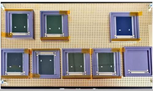
The objective of the activity is the design, manufacture and characterisation of a CMOS image sensor based on high-resistivity epitaxial silicon.
Description
Visible image sensors with high sensitivity extending into the Near Infrared (NIR) are in high demand for many planned and future Earth observation and Science missions. The benefits of high-resistivity silicon in this area for CCDs has been previously demonstrated.
The aim of this activity is to extend these benefits to CMOS image sensors and subsequently exploit the enhanced read-out capabilities and radiation tolerance which are inherent to CMOS image sensors.
The benefits of the developed technology will be:
Better electro-optical performance will be achieved, due to the use of thicker starting material e.g. increased Quantum Efficiency (QE) at higher energies (above ~3keV) or at long wavelengths (NIR).
The possibility to achieve improved MTF performance by using appropriate processes and controlling the photodiode depletion with respect to the total thickness of the material.
Emphasis shall be given to the schematic representation of the pixel layout as well as detailed detector architecture with schematics at transistor level of the main building blocks including pixel, column amplifier, programmable gain amplifier (if applicable), multiplexer and output amplifier. The pixel design with a schematic representation of metal layers and diffusion areas etc is expected to be based on detailed simulations and modelling of predicted performance.
The following tasks will be done in the frame of this activity:
Detector specification and trade-off study.
Preliminary detector design and pixel simulation.
Detailed detector design.
Detector manufacture.
Detector characterization including radiation testing.
Evaluation, conclusions and recommendations.
• Application domain: Generic Technologies
•
Technology Domain:
17 - Optoelectronics
17 - Optoelectronics
•
Competence Domain:
1-EEE Components, Photonics, MEMS
1-EEE Components, Photonics, MEMS
• Initial TRL: TRL 3
• Target TRL: TRL 4
•HarmoRoadMap: Optical Detectors, Visible Range (2015.1)
•IPC Document: ESA/IPC(2018)61||ESA/IPC(2020)61,add.6