De-risk assessment: 3D screen printing for high frequency devices implemented in Groove Gap Waveguide technology
Programme Reference
G617-241TAjf
Status
Closed
Country
Germany
Start Date
2023
End Date
2025
Programme: GSTP Prime Contractor: Fraunhofer Gesellschaft
Subcontractors:
CHRISTIAN-ALBRECHTS-UNIVERSITAET ZU KIEL • Germany
Objectives
The goal was to develop a reliable manufacturing route for GGW (Groove Gap Waveguide) components, using the 3D screen printing process to achieve high resolution, good surface finish, and precise geometrical accuracy. This was particularly important for the high-frequency applications targeted by the project, where even minor deviations in component dimensions can significantly affect performance.
Description
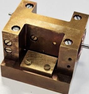
The project included the design, fabrication, and characterization of key components such as transmission lines, resonators, and third-order filters in GGW technology. These components were manufactured using 3D screen printing and then subjected to rigorous testing to validate their electrical and geometric properties. A key technical challenge was to maintain dimensional tolerances within ±15 µm and surface roughness (Ra) below 3 µm to ensure optimal performance at high frequencies.The project successfully established a 3D screen printing process for GGW structures. This additive manufacturing technique was shown to be suitable for creating high-precision components with fine features, such as cylindrical pins used in the GGW architecture. A key advantage of 3D screen printing over other additive processes is its ability to produce components with smooth surfaces and low roughness, which is critical for reducing losses in high-frequency devices.
• Application domain: GEN-Generic Technologies
•
Technology Domain:
24-Materials and Manufacturing Processes
24-Materials and Manufacturing Processes
•
Competence Domain:
2-Structures, Mechanisms, Materials, Thermal
2-Structures, Mechanisms, Materials, Thermal
• Initial TRL: TRL 3
• Target TRL: TRL 4
• Achieved TRL: TRL 4
•HarmoRoadMap: N/A
•IPC Document: N/A
•Public Document: