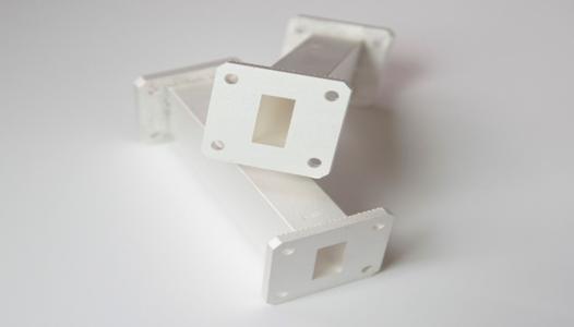
Autocatalytic Silver for Space Applications
Programme Reference
G617-204QT
Status
Closed
Country
Sweden
Start Date
2017
End Date
2019
Programme: GSTP Prime Contractor: RISE IVF AB
Objectives
The objective of this activity is to develop and verify the possibility to use the autocatalytic silver process for space applications, such as a final finish for PCBs and as a conductive layer for microwave components. The aim is to optimise and industrialise the process for the targeted applications.
Description
Autocatalytic silver is an alternative to electroplating processes and it has the potential to improve both performance and reduce plating costs. The autocatalytic nature of the process means that plating is continued as long as the substrate is immersed in the plating bath, providing the unique feature of unlimited silver-film thickness without applying a current to the substrate. ASIG (Autocatalytic Silver Immersion Gold) was developed primarily as an alternative surface finish for chip packaging substrates, and the process became commercially available in 2010. For PCBs, ASIG has been developed as a replacement for nickel based surface finishes which are known to suffer from quality issues, such as brittle intermetallics or blackpad failures. For space use, the two most important applications are, microwave components and final surface finish for soldering of PCBs. Examples of other applications for autocatalytic silver are silicon wafers, solar cells, semiconductors and plating on plastics. ASIG is also excellent from RF-perspective, especially for high speed applications, since copper and silver have the closest resistivity at 1.5 and 1.6 micro-ohm cm and are thus the least lossy. The ASIG process is today in commercial use for production of PCB's for gold wire bonding applications. For microwave components, the technology gives excellent possibilities to reduce insertion loss and passive intermodulation (PIM) for typical microwave components, such as wave guides, filters, corrugated horns, manifolds, diplexers etc., by the ability to plate complex geometries, larger segments, and narrow dimensions with small thickness variations. The traditional electroplating has a limited ability to plate in complex geometries, especially if there is a need to put anodes into very narrow cavities. Therefore, improved productivity and enhanced RF-performance can be gained if more complex components could be plated. The activity proposed will profit from the results and lessons learned in prior lower TRL development activity (Electroless Silver) in which a unique autocatalytic electroless silver process was tested for PCB applications, microwave component applications and for plastic applications. Further optimization of the process was foreseen, in order to verify the process for space applications. This activity shall cover the following tasks: Develop and optimize the process in laboratory scale with the aim to fulfil space demands of surface properties and plating coverage for PCBs and microwave component applications Demonstrator parts shall be manufactured and tested (via a dedicated verification test campaign) to demonstrate success in meeting the applications requirements (including e.g. simulation of storage, assessment of solderability, reliability testing of solder joints and Rfperformance) Evaluation of technology demonstrator samples to verify the proposed plating technology and thickness requirements in order to ensure that autocatalytic silver coatings will meet both PCB surface requirements and RF requirements for microwave components After the demonstrator samples have been successfully evaluated, the technology shall be applied on test coupons with different geometrical features to demonstrate the ability to plate complex geometries for microwave components Quality control shall be demonstrated in order to meet space environment requirements for flight representative PCBs and microwave components ; ; (change ESA/IPC(2019)61) It is proposed to change the budget, scope and duration of this activity. ; The reason for the change is to improve the electrical performance compared with machined surfaces on waveguides. ; Therefore, the additional work to be performed will be the application of autocatalytic silver onto 3D-printed aluminium waveguides, which will include 3D-printing of waveguides, process optimisation and plating of the printed waveguides and evaluation testing of the plated waveguides. In particular, the additional tasks to be done are the following: Test sample design and test planning, Manufacturing of test samples, Evaluation testing of silver plated samples, Final reporting and conclusions ;
• Application domain: Generic Technologies
•
Technology Domain:
24 - Materials and Manufacturing Processes
24 - Materials and Manufacturing Processes
•
Competence Domain:
2-Structures, Mechanisms, Materials, Thermal
2-Structures, Mechanisms, Materials, Thermal
• Initial TRL: TRL 3
• Target TRL: TRL 5
• Achieved TRL: TRL N/A
•HarmoRoadMap: N/A
•IPC Document: ESA/IPC(2015)61,add.6||ESA/IPC(2019)61
•Public Document:

