De-risk assessment: Implementation of Sum-Int ADC IP-core into radiation-tolerant FPGA and performance evaluation
Programme Reference
G617-241TAfj
Status
Closed
Country
Czech Republic
Start Date
2021
End Date
2022
Programme: GSTP Prime Contractor: PIKRON, S.R.O.
Objectives
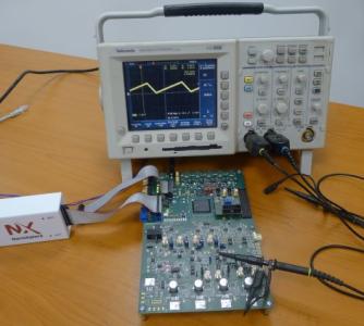
The primary objectives of the activity are verification of suitability of PiKRON's company original architecture of Analog-to-Digital Converter (ADC) for use in combination with radiation-tolerant FPGA (nanoXplore NG MEDIUM BRAVE chosen) and preparation of open-source design files which allows a synthesis of the converter control logic for multiple resolutions and sample rates according to requirements of the actual target applications. The design is already used together with consumer grade FPGAs and requires only a single external op-amp per channel and two digital I/O pins on FPGA for resolution about 12 bits. PiKRON uses the Sum-Int conversion technique even for high resolution (20 bits) applications in High Performance Liquid Chromatography (HPLC) spectrophotometric detectors. The precise (chopper stabilized) amplifiers, analog switches and comparator were required for such use. Some The secondary objective is to use developed platform for experiments which allow porting of PiKRON's motion control (PMSM, DC and stepper motors) solutions based on the Sum-Int ADC technique for the winding current sensing to the space-qualified components in future. The main goal, minimal components realization on space-grade FPGA, has reached committing criteria. Advantages and found limitations of the solution are described in the technical and conclusion parts of this activity.
Description
The main advantage of the proposed design of middle resolution class analog to digital conversion for space application is minimal demand for additional special function/parameters components (single middle class op-amp, resistors and capacitor are enough). All other required functionality, including analog signal comparator and reference switching, can be implemented in FPGA digital subsystem for middle resolution range applications. This makes the choice of space mature/proven components easier. The design provides continuous source signal measurement with zero theoretical quantification error accumulation over multiple samples. The principle of operation has advantages over classical sigma-delta ADC: significantly lower number of reference source switching and constant mean frequency of the reference source switching.
• Application domain: Generic Technologies
•
Technology Domain:
1 - On-board Data Subsystems
1 - On-board Data Subsystems
•
Competence Domain:
3-Avionic Systems
3-Avionic Systems
• Initial TRL: TRL N/A
• Target TRL: TRL N/A
•HarmoRoadMap: N/A
•IPC Document: N/A
•Public Document: